Often, when building a guitar tube amp, not enough of a triode for the cathode follower, which is loaded on the tonestack. There is thought to use for this high voltage mosfet. It would seem, may be pitfalls in the follower? In this case, is not so simple. First, consider the work of the cathode follower, which is loaded on the tonestack.

RE и CE – the equivalent resistance and capacitance of the tonestack.
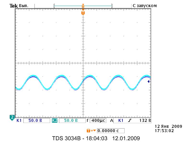
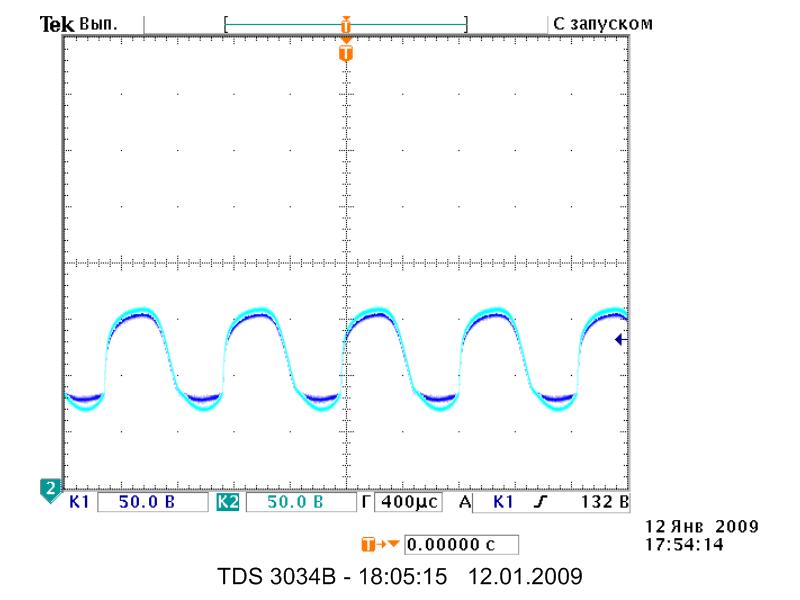
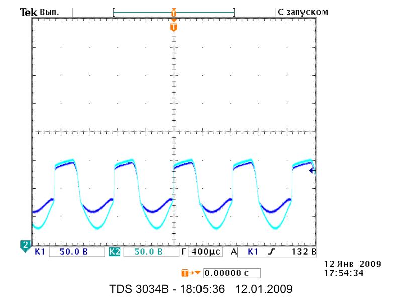
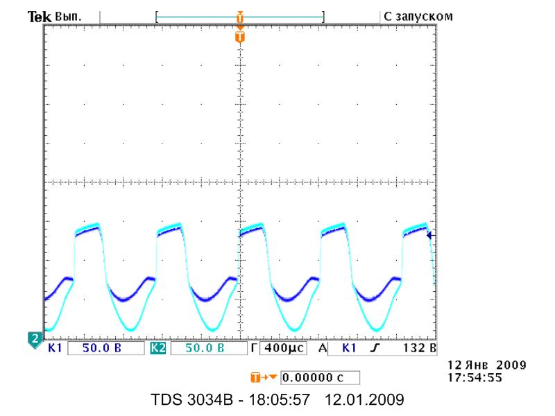
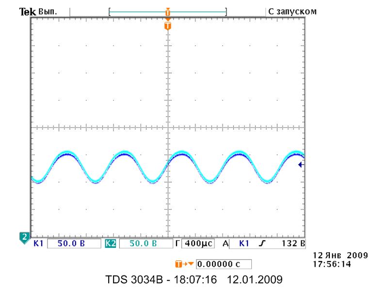
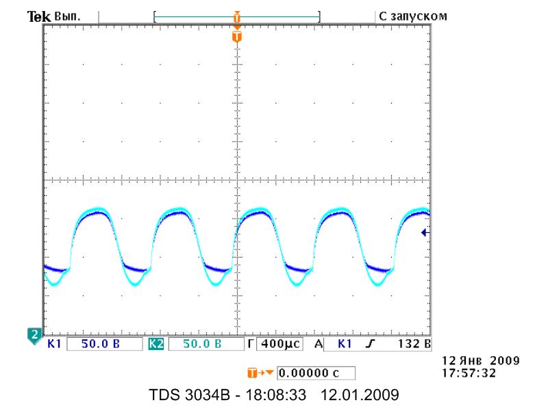
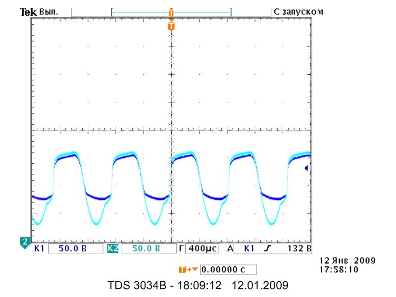
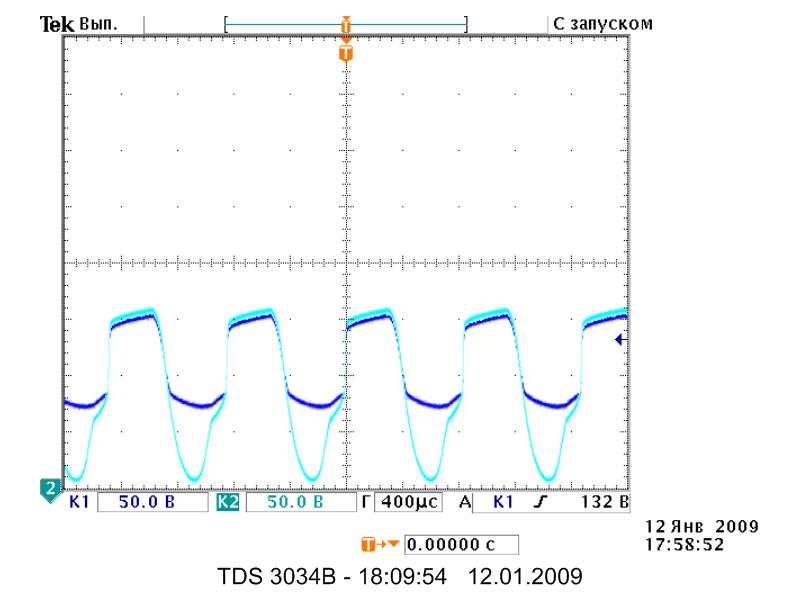
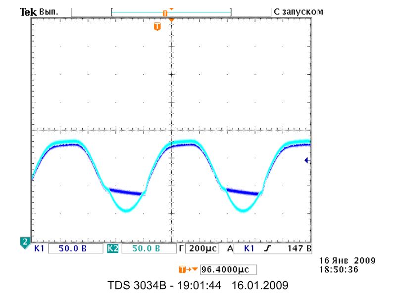
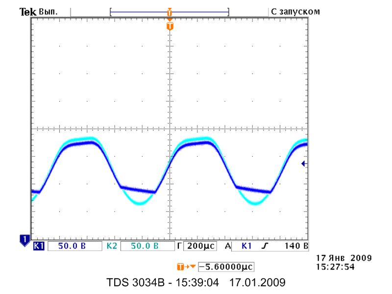
Oscillograms of the output, with the progressive increase in amplitude of the input voltage of the cathode follower (hereinafter for brevity, CF).
Dark blue color shows the input signal of follower (anode V1.A), light blue - the voltage on R3.


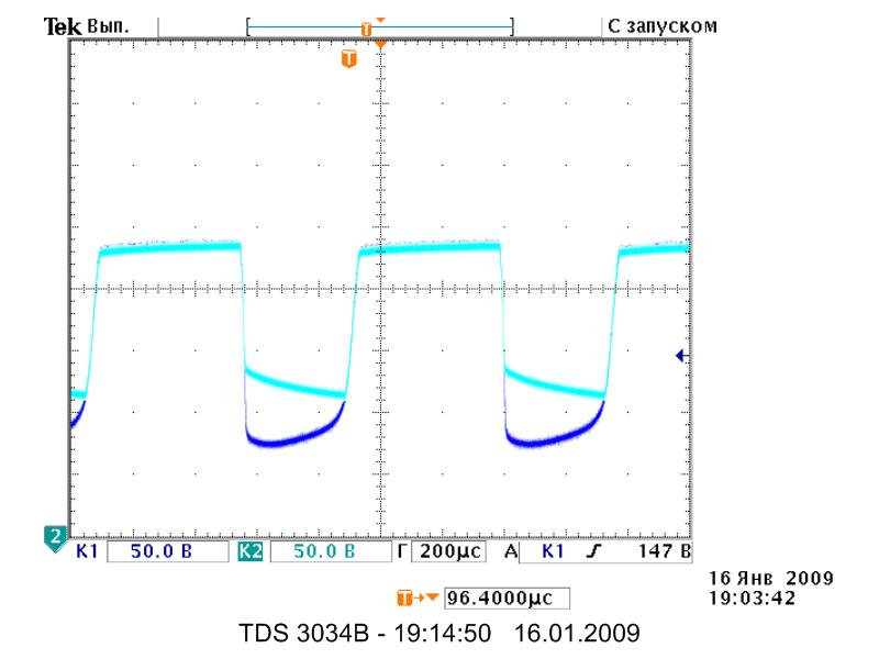
You can notice two things. The first - on top of the upper half-wave begins rounding, passing in an inclined slant due to the fact that the CF goes into the grid current limiting mode, becoming almost vacuum diode. The second - an unusual diagonal slope of the lower half-wave, unlike the common cathode stage grid current limit. He is due to the fact that at the upper half-wave tonestack capacitors are charged to a voltage comparable with the voltage of the cascade supply. When going down the signal reach point when the voltage at the cathode will be equal to the voltage accumulated on the CE divided in the ratio R3 / RE. At this point, occurs the fixation on the cathode voltage, as well as the grid continues to go down after the signal goes into cathode current cutoff and actually turned off from work. Bottom slope - no more than a discharge CE through R3-RE.
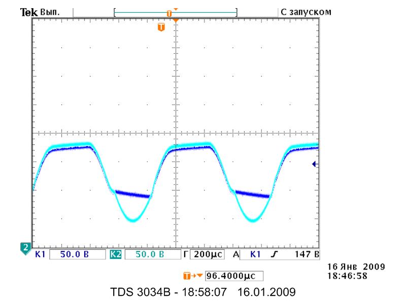
Now, consider the source follower (hereinafter for brevity, SF).

Standard connection, SW1 - is On, SW2 - is Off, PT1 = 0 Ohm

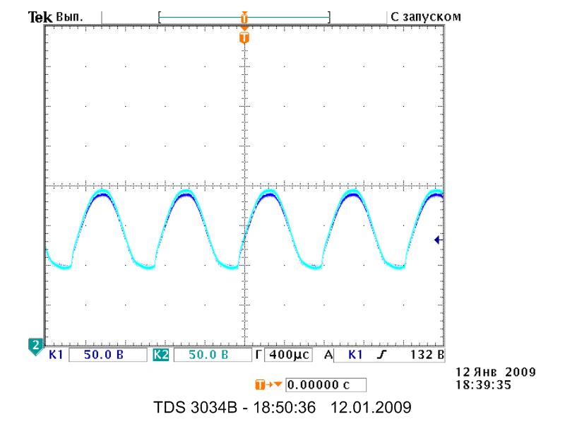

No grid current limit on the upper half wave. On the bottom half wave observe the following pattern on R3: first comes current cutoff, and then the signal starts to go down, after the input signal. This is work of protective gate-source zener, although in some datasheets about it, nothing is written! Although if it was not exists, the gate would be broken, because the maximum gate-source voltage for the majority mosfets ± 20-25V, and the gate-source voltage difference can be up to 100 V of reverse voltage.
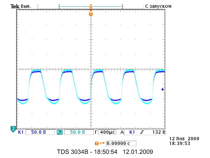
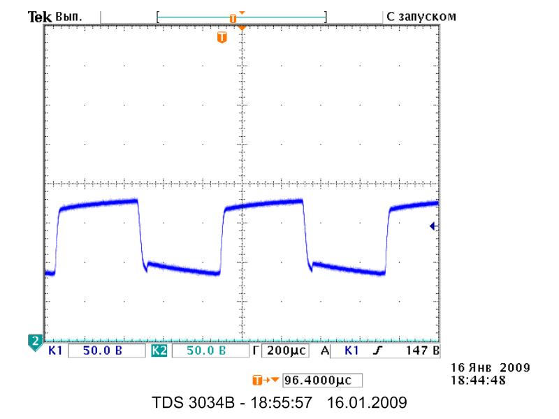
Emulation of the CF grid current , SW1 - is On, SW2 - is On. PT1 adjucting ensures that at the top of the signal D2 opened, preventing further increase in gate-source voltage than actually achieved emulation of the CF grid current.

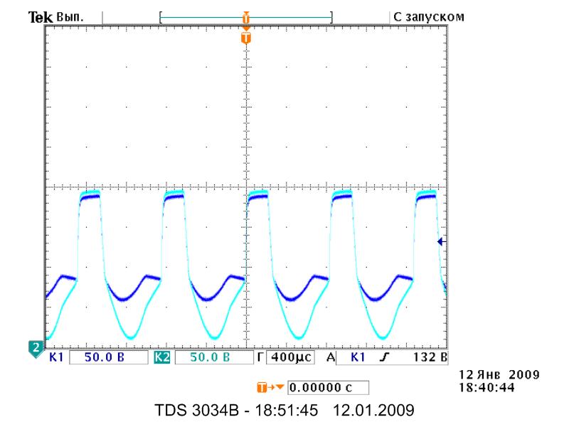
Emulation of the CF grid current and the cutoff, SW1 - is Off, SW2 - if On. R2 serves to reduce the penetration of the signal through a protective zener to output. D1 serves to preserve the possibility of emulation of CF grid current.

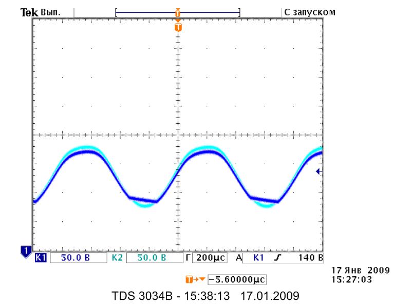
After discussion with Mikhail Semyonov (OldMike), was born, another schematics.

First, D3 was not, and it added later.


At the last waveform is clearly visible tooth, which is formed by differentiation of signal on the D1 capacitance.
After adding D3 problem was solwed.


Diode D1 should have a maximum reverse voltage of more then stage supply as well as the for D3 used pulsed diode with a minimum capacitance.
D2 gate-source zener also protects the gate from the breakdown at high reverse voltages, fixing the reverse voltage at 0.6 V.
Some notes about adjusting circuit without an oscilloscope. Remove the tube before the follower (V1 in my schematics) and by adjucting PT1 seek to voltage on the load (cathode D3 in my schematics) was by 40-60 in less than the stage supply voltage.